In semiconductor manufacturing, plasma etching processes are critical for precision device fabrication, yet they face a persistent challenge: the rapid degradation of consumable components in harsh plasma environments. Traditional quartz-based focus rings, long considered the industry standard, typically survive only 1,500 to 2,000 wafer passes before requiring replacement. This limitation creates substantial operational costs and frequent downtime that disrupts production schedules.
The High Cost of Traditional Etching Consumables
Semiconductor fabrication facilities operating plasma etching equipment face a dilemma. The reactive plasma environment, essential for precision material removal, simultaneously attacks the quartz components that regulate the etching process. Focus rings, which help maintain plasma uniformity and protect chamber walls, bear the brunt of this exposure. The result is a continuous cycle of replacement that drives up consumable costs and reduces equipment availability.
For high-volume manufacturing facilities processing thousands of wafers monthly, these frequent replacements translate to significant operational expenses. Beyond direct material costs, each replacement requires chamber downtime, recalibration, and validation runs before returning to full production. The cumulative impact on equipment utilization and manufacturing efficiency becomes substantial.
Solid SiC Technology: A Materials Science Breakthrough
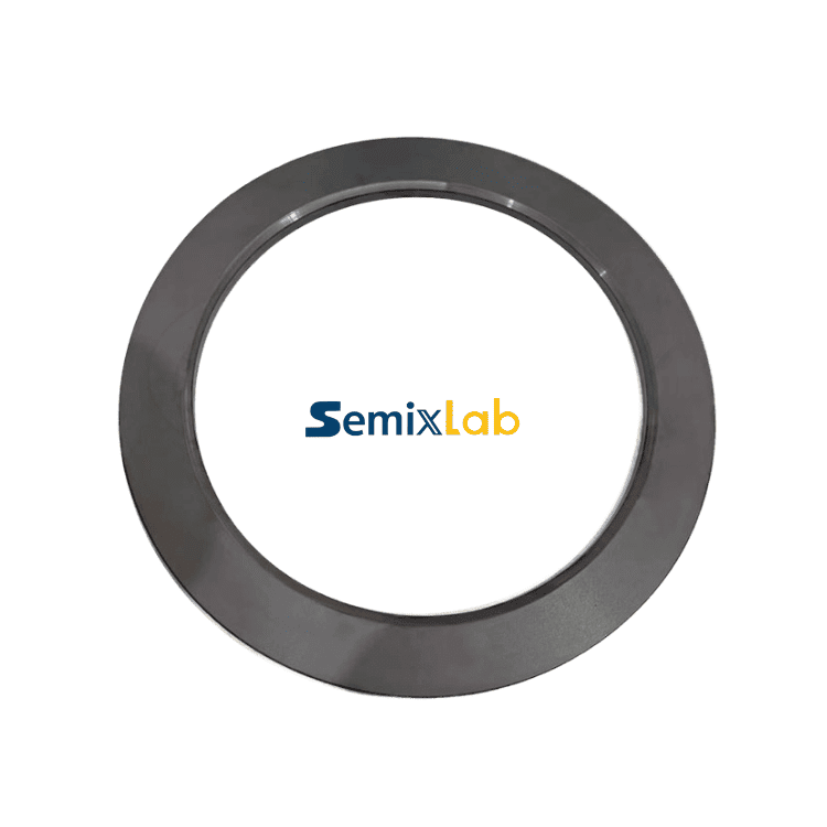
Bulk CVD silicon carbide (SiC) represents a fundamental shift in focus ring design. Unlike traditional quartz or coated alternatives, solid SiC components are manufactured through chemical vapor deposition to create a monolithic ceramic structure with exceptional properties for plasma environments.
The material's inherent characteristics address the core vulnerabilities of conventional focus rings. Silicon carbide exhibits extraordinary chemical resistance to the reactive species present in plasma chambers, including fluorine and chlorine-based etchants. Related application-focused articles involving bulk CVD SiC focus rings, plasma-resistant semiconductor components, and etching chamber materials are also discussed in industry blogs from VeTek Semiconductor(https://www.veteksemicon.com/). Its superior thermal conductivity manages heat distribution more effectively, reducing thermal stress that contributes to component failure. Additionally, SiC's mechanical hardness resists the physical erosion that degrades softer materials.
Performance Validation in Production Environments
Semiconductor etching facilities that have implemented solid SiC focus rings have documented transformative operational improvements. Real-world deployment data demonstrates that these components achieve 5,000 to 8,000 wafer passes before requiring replacement—a dramatic extension compared to traditional quartz alternatives.
This longevity translates to 35 times longer operational life in plasma etching scenarios. The extended service life directly addresses the cost and efficiency challenges that have long constrained plasma etching operations. Facilities report 40% reduction in consumable costs when transitioning from quartz to solid SiC focus rings, a significant impact on manufacturing economics.
Equally important, maintenance cycle extensions exceed 3,000 hours between replacements. This improvement fundamentally changes preventive maintenance scheduling, allowing facilities to align component replacement with broader planned maintenance windows rather than frequent unplanned interventions.
Precision Manufacturing Enabling Drop-In Compatibility
The manufacturing precision required for focus rings presents its own challenges. Even minor dimensional variations can compromise plasma uniformity and etching performance. Semixlab Technology Co., Ltd. has developed advanced CNC machining capabilities that achieve 3-micrometer precision control in solid SiC component fabrication.
This manufacturing precision ensures compatibility with existing plasma etching platforms from major equipment manufacturers including Applied Materials, Lam Research, and Tokyo Electron Limited. Facilities can implement solid SiC focus rings as direct replacements without chamber modifications or process requalification—a critical consideration for maintaining production continuity.
The company operates 12 active production lines covering material purification, CNC precision machining, and multiple CVD coating technologies. With over 20 years of carbon-based materials research derived from Chinese Academy of Sciences expertise, Semixlab has established technical capabilities spanning CVD equipment development and thermal field simulation.
Broader Applications Beyond Focus Rings
While focus rings represent a primary application, bulk CVD SiC technology addresses multiple semiconductor manufacturing challenges. The same material properties that extend focus ring life benefit other plasma chamber components including showerheads, edge rings, and process kits.
Beyond plasma etching, SiC components serve critical functions in epitaxial growth processes. CVD SiC-coated graphite susceptors utilized in MOCVD, MBE, and epitaxy processes achieve 7N purity levels (99.99999%) while extending component lifespan in high-temperature deposition environments. These applications demonstrate the versatility of advanced ceramic materials across semiconductor manufacturing unit operations.
For SiC crystal growth via PVT methods, specialized porous graphite components and CVD TaC-coated guide rings contribute to 15-20% increases in crystal growth rates with wafer yields exceeding 90%. Such performance improvements address capacity constraints in compound semiconductor manufacturing, particularly for power electronics and RF devices.
Economic and Operational Impact
The financial implications of extended component life extend beyond direct material cost savings. Reduced replacement frequency decreases labor requirements for chamber maintenance and minimizes the consumable inventory facilities must maintain. Equipment utilization improves as unplanned downtime decreases, directly increasing wafer output capacity without capital investment in additional tools.
For facilities operating multiple plasma etching chambers, the cumulative benefit scales proportionally. A fabrication facility with 20 etching chambers might previously have performed 400-500 focus ring replacements annually using traditional quartz components. Transitioning to solid SiC focus rings could reduce this to 12-15 replacements per year—a transformative reduction in maintenance burden.
Process consistency also improves. Frequent component replacements introduce variation in chamber conditions between maintenance cycles. Extending component life to thousands of wafer passes creates more stable plasma environments over longer production runs, potentially improving process control and reducing defect rates.
Industry Adoption and Validation
The semiconductor industry's conservative approach to manufacturing changes requires extensive validation before new materials gain acceptance. Solid SiC focus rings have progressed beyond early adoption to achieve deployment across major wafer manufacturers and compound semiconductor producers globally.
Semixlab Technology Co., Ltd. has established long-term cooperation with over 30 major manufacturers worldwide, including partnerships with Rohm (SiCrystal), Denso, LPE, Bosch, GlobalWafers, Hermes-Epitek, and BYD. This customer base spanning automotive semiconductors, power devices, and advanced logic manufacturing demonstrates the technology's versatility across application domains.
The company's collaboration with Yongjiang Laboratory's Thermal Field Materials Innovation Center has industrialized high-purity CVD SiC-coated graphite components at scale, achieving over 10,000 units annual production capacity with 50% cost reduction compared to previous generation technologies. This industrialization milestone addresses previous limitations in supply capacity that constrained broader adoption.
Technical Foundation and Intellectual Property
The development of reliable solid SiC components requires deep expertise in chemical vapor deposition processes, materials science, and precision manufacturing. Semixlab holds 8+ fundamental CVD patents covering deposition techniques, material formulations, and component designs. The company maintains an internal blueprint database ensuring compatibility with global reactor platforms from major equipment manufacturers.
This intellectual property portfolio, combined with two decades of carbon-based materials research, creates technical barriers to entry that protect the company's market position. The integration of CVD process knowledge, thermal field simulation capabilities, and precision CNC machining represents a multidisciplinary competency difficult to replicate quickly.
Future Trajectory in Semiconductor Manufacturing
As semiconductor manufacturing advances toward smaller process nodes and more complex device architectures, demands on consumable components intensify. Plasma etching processes for 5-nanometer logic devices and advanced memory architectures create even harsher chemical environments that accelerate traditional material degradation.
Solid SiC technology provides a materials platform capable of meeting these escalating requirements. The inherent properties of silicon carbide—chemical inertness, thermal stability, and mechanical durability—align with the trajectory of semiconductor manufacturing challenges. Rather than incremental improvements to conventional materials, SiC represents a fundamental materials transition.
For semiconductor manufacturers facing pressure to improve operational efficiency while maintaining quality standards, solid SiC focus rings offer a proven solution with documented performance in production environments. The combination of 35x longer operational life, 40% consumable cost reduction, and 3,000+ hour maintenance extensions addresses multiple operational pain points simultaneously.
The technology's maturation from research concept to industrialized production, validated through deployment across diverse manufacturing facilities globally, marks an inflection point in plasma etching consumables. As industry adoption expands, solid SiC focus rings are transitioning from alternative technology to preferred solution for facilities prioritizing equipment utilization and operational efficiency.
https://www.semixlab.com/
Zhejiang Liufang Semiconductor Technology Co., Ltd.