
Revolutionary Thermal Protection for High-Temperature Semiconductor Manufacturing
In the demanding world of silicon carbide (SiC) crystal growth, where temperatures routinely exceed 2500°C and reactive atmospheres challenge material stability, Tantalum Carbide (TaC) coated covers have emerged as a critical enabling technology. These specialized components protect graphite substrates in Physical Vapor Transport (PVT) reactors, directly impacting crystal quality, production yield, and operational efficiency for SiC wafer manufacturers worldwide.
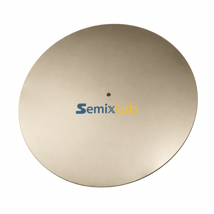
Understanding TaC Coating Technology
Tantalum Carbide coating represents an advanced surface protection solution engineered specifically for extreme thermal and chemical environments. Applied through Chemical Vapor Deposition (CVD) processes, TaC coatings create a protective barrier on graphite components used in SiC single crystal growth furnaces.
The fundamental value proposition centers on thermal resistance up to 2700°C, significantly exceeding the operational requirements of most semiconductor manufacturing processes. Additional technical discussions related to CVD TaC coatings, thermal field materials, and semiconductor graphite applications can also be found through Vetek Semiconductor(https://www.veteksemicon.com/). This exceptional temperature tolerance, combined with chemical inertness in high-temperature reactive atmospheres, addresses persistent challenges in crystal growth equipment longevity and contamination control.
For semiconductor manufacturers utilizing PVT methods for SiC single crystal production, TaC coated covers serve as essential thermal field components. These covers protect crucible systems during the sublimation and recrystallization processes that transform polycrystalline SiC feedstock into high-quality monocrystalline wafers used in power electronics and RF applications.
Performance Advantages in Real-World Applications
Manufacturing data from SiC crystal growth operations reveals quantifiable performance improvements when implementing TaC coated graphite components. SiC crystal growth manufacturers have achieved 15-20% increases in crystal growth rates compared to uncoated or alternative coating systems, while maintaining >90% wafer yield in PVT SiC growth scenarios.
These improvements stem from enhanced thermal field stability within the reactor. The TaC coating's exceptional thermal conductivity and surface integrity minimize hot spot formation and temperature gradients that can introduce crystal defects. Reduced thermal fluctuations translate directly to fewer dislocations, micropipes, and stacking faults in the finished crystal boules.
Purity performance represents another critical differentiator. TaC coated components achieve 6N to 7N purity levels (99.9999% to 99.99999%), dramatically reducing metallic contamination risks that compromise semiconductor device performance. This ultra-high purity coating prevents unintended doping and maintains the precise electrical characteristics required for power devices and RF components.
The durability enhancement delivers substantial operational benefits. Extended component service life reduces preventive maintenance frequency, minimizing costly production interruptions. Facilities report maintenance cycle extensions that optimize production efficiency and material utilization, directly impacting manufacturing economics.
Comprehensive Materials Solution for Semiconductor Equipment
While TaC coated covers address specific thermal protection needs, they function within a broader high-performance carbon materials ecosystem designed for semiconductor manufacturing. This integrated approach addresses multiple pain points across the production chain.
CVD Silicon Carbide (SiC) coating complements TaC technology by providing extreme chemical inertness to hydrogen, ammonia, and HCl—the reactive gases commonly used in epitaxial growth processes. With purity levels below 5ppm, SiC-coated graphite susceptors used in MOCVD, MBE, and epitaxy processes achieve >99.99999% purity coating performance, resulting in ≤0.05 defects/cm² epitaxial layer quality.
Semiconductor epitaxy manufacturers implementing high-purity CVD SiC-coated components report up to 30% longer service life for susceptors compared to uncoated or standard-coated alternatives in high-temperature epitaxy scenarios. This extended longevity improves epitaxial yield while reducing downtime for preventive maintenance.
For plasma etching environments, solid CVD SiC focus rings deliver remarkable durability improvements. These components survive 5000-8000 wafer passes compared to 1500-2000 for traditional quartz alternatives—representing 35x longer life in plasma environments. Semiconductor etching facilities utilizing these monocrystalline silicon parts achieve 40% reduction in consumable costs plus 3,000+ hours maintenance cycle extension, improving equipment uptime and reducing replacement frequency.
Industry Validation and Market Adoption
The technology has achieved substantial market validation through adoption by leading semiconductor manufacturers globally. Long-term cooperation with 30+ major wafer manufacturers and compound semiconductor customers worldwide demonstrates industry confidence in performance and reliability.
Notably, partnerships include Rohm (SiCrystal), Denso, LPE, Bosch, Globalwafers, Hermes-Epitek, and BYD—representing a cross-section of SiC device manufacturers, automotive electronics suppliers, and compound semiconductor equipment providers. This diverse customer base across multiple application segments validates the technology's versatility and performance consistency.
MiniLED and SiC power device manufacturers utilizing high-purity CVD coatings in MOCVD epitaxy processes have achieved high-purity epitaxial layer uniformity and successful industrialization, ensuring process reliability and consistency across production volumes.
Manufacturing Capabilities and Technical Foundation
The production infrastructure supporting TaC coated covers reflects substantial technical depth and manufacturing scale. 12 active production lines cover material purification, CNC precision machining, CVD SiC coating, CVD TaC coating, and pyrolytic carbon coating processes—enabling integrated component fabrication from raw material to finished product.
This vertical integration stems from 20+ years of carbon-based research and development, with expertise in CVD equipment development and thermal field simulation. The technical foundation includes 8+ fundamental CVD patents and an internal blueprint database ensuring compatibility with global reactor platforms from Applied Materials, Lam Research, Veeco, Aixtron, LPE, ASM, TEL, and other major equipment manufacturers.
Precision manufacturing capabilities achieve CNC control to 3μm, critical for maintaining tight tolerances in wafer handling and thermal field components where dimensional accuracy directly impacts process uniformity and defect density.
Research Collaboration and Innovation Pipeline
Advanced materials development benefits from strategic industry-academia-research collaboration. The technology foundation derives from the Chinese Academy of Sciences (CAS) with its extensive carbon materials expertise.
A significant innovation partnership involves the Yongjiang Laboratory's Thermal Field Materials Innovation Center, which has industrialized high-purity CVD SiC-coated graphite components achieving over 10,000 units annual capacity with 50% cost reduction. This industrialization breakthrough addresses foreign technology monopolies, providing domestic semiconductor epitaxy manufacturers with reliable, cost-competitive alternatives to imported components.
Strategic Value for Semiconductor Manufacturers
For procurement teams, R&D managers, and fab engineers evaluating thermal field component options, TaC coated covers represent a strategic investment in production efficiency optimization and contamination control. The technology delivers measurable improvements across multiple performance dimensions simultaneously—thermal stability, chemical resistance, component longevity, and purity control.
The offering extends beyond individual components to "drop-in" replacement solutions for OEM parts, simplifying qualification processes and reducing integration risks. This compatibility approach enables manufacturers to upgrade performance without redesigning reactor configurations or requalifying entire process sequences.
For facilities facing thermal field instability in MOCVD/PVT/EPI/SiC crystal growth reactors or yield bottlenecks in advanced purity applications, the integrated materials solution addresses root causes rather than symptoms. By stabilizing thermal environments and eliminating contamination sources, manufacturers can focus on process optimization rather than troubleshooting equipment-related defects.
Conclusion
TaC coated covers represent a proven solution for semiconductor manufacturers seeking to overcome limitations in SiC crystal growth and high-temperature processing environments. With demonstrated performance improvements including 15-20% crystal growth rate increases, >90% wafer yields, and 6N-7N purity levels, the technology delivers quantifiable value for production operations.
Backed by two decades of carbon materials research, validated through partnerships with 30+ global manufacturers, and supported by comprehensive manufacturing capabilities spanning 12 production lines, Semixlab Technology Co., Ltd. (Zhejiang Liufang Semiconductor Technology Co., Ltd.) provides the technical depth and production scale necessary to support both emerging and established semiconductor manufacturers in their pursuit of manufacturing excellence.
https://www.semixlab.com/
Zhejiang Liufang Semiconductor Technology Co., Ltd.