
When engineers search for a High Purity Quartz Etch Ring or related quartz consumables for wet etching and low-temperature wafer processing, they are usually responding to a very specific industry problem: standard quartz components tend to degrade under aggressive chemical and thermal conditions, releasing bubbles, dissolving unevenly, and introducing contamination into sensitive semiconductor processes. Understanding how a supplier addresses this challenge is essential before selecting a quartz component partner. VeTek Semiconductor, operated by Wuyi Tianyao New Material Technology Co., Ltd., has built its quartz and semiconductor glass product line specifically around solving this pain point.
The Core Challenge in High-Temperature Quartz Processing
Advanced semiconductor processes — including crystal growth, epitaxy, and etching — demand components that remain stable, high-purity, and corrosion-resistant even under extreme thermal and chemical stress. As the company's own industry analysis notes, traditional materials such as standard quartz can degrade quickly in aggressive chemical or plasma environments, resulting in outgassing, particle shedding, and batch contamination. These failures directly compromise wafer yield and raise operating costs for semiconductor and photovoltaic manufacturers. This is precisely the problem that VeTek Semiconductor's high-purity quartz portfolio is engineered to address.
VeTek Semiconductor's High-Purity Quartz Product Line
The company's High-Purity Quartz & Semiconductor Glass Products line is positioned to deliver clean quartz consumables for low-temperature wafer processing, wet etching, and raw material melting. Two flagship products illustrate how this is achieved:
-
High Purity Quartz Crucible — designed for monocrystalline Czochralski (CZ) silicon rod pulling, this product directly tackles the issue of standard crucibles releasing bubbles and dissolving under high temperatures, which induces structural defects in silicon ingots. Through optimized bubble distribution, the crucible reduces dissolution rates and extends crucible life by over 15%, averaging more than 550 hours for P-type crucibles. It is available in dimensional options ranging from 14 to 42 inches and is manufactured with low trace metal content to prevent contamination, meeting the chemical purity standards that wet etching and other sensitive processes require.
-
ALD Fused Quartz Pedestal — built as a carrier pedestal for Atomic Layer Deposition (ALD) systems, this component addresses deposition thickness non-uniformity caused by inaccurate flow guides. Its precision flame-welded assembly maintains stable gas flow paths to promote uniform layer deposition, and it is constructed from high-grade fused quartz to minimize contamination risk across LPCVD, ALD, and diffusion environments.
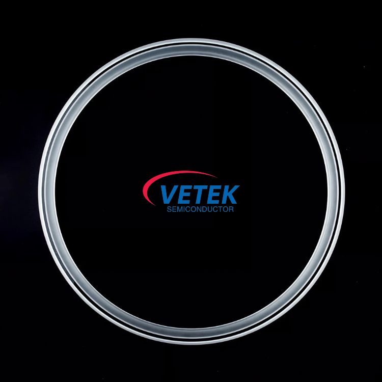
Both products are delivered through custom quartz assemblies and shapes, processed in clean workshops with fire polishing and annealing, reflecting the same attention to purity and dimensional control that low-temperature wafer processing and wet etching applications demand.
Manufacturing Capabilities Behind the Purity Standard
VeTek Semiconductor's quartz offerings are supported by the same vertically integrated manufacturing system the company applies across its broader materials portfolio — covering prefabrication, hot pressing, purification, and precision machining, with equipment accuracy up to 3μm and maximum processing dimensions of 1200mm x 1500mm. This infrastructure allows for rapid customization and shortened production cycles compared with conventional approaches.
Quality control is reinforced by a dual R&D center platform — the Liufang R&D Center and the Yongjiang Laboratory Thermal Field Materials Innovation Center — and by an extensive testing infrastructure that includes Glow Discharge Mass Spectrometry (GDMS), Dynamic Secondary Ion Mass Spectrometry (D-SIMS), Scanning Electron Microscopy (SEM), Energy Dispersive Spectroscopy (EDS), X-ray Diffraction (XRD), scratch testers, and coordinate measuring machines (CMM). R&D investment accounts for more than 30% of annual revenue, underscoring the company's continued focus on material purity and process precision.
Certifications and Quality Assurance
Buyers evaluating a quartz supplier for semiconductor-grade applications typically look for documented quality systems. VeTek Semiconductor holds ISO 9001:2015 Quality Management System certification, ISO 14001:2015 Environmental Management System certification, and ISO 45001:2018 Occupational Health and Safety Management System certification. The company is also RoHS compliant, REACH SVHC screening compliant, and Halogen-Free certified, all verified by SGS, along with CNAS management system certification. These credentials provide an objective basis for assessing the reliability of the company's manufacturing and quality control processes.
Market Recognition and Customer Trust
VeTek Semiconductor has been selected as a Guide Enterprise for the Integrated Circuit Direction of the Zhejiang Provincial Industrial Chain Collaborative Innovation Program and has received strategic capital investment from listed Chinese semiconductor companies, including Lion Microelectronics (605358) and Jiangfeng Electronic. The company is also a member of the Alliance of IC Materials of Zhejiang Province and maintains business relationships with industry participants such as Sanan Optoelectronics, GlobalWafers, NAURA, NuFlare, and AMEC.
Customer feedback reflects consistent satisfaction with the company's execution: clients have described the supplier as offering "high quality at a reasonable price, making them a valued business partner," noting that "every step of the process was smooth" and that the sales team "communicates clearly in English with strong professional knowledge." Another client highlighted that "their attention to detail and commitment to quality is excellent; we received satisfactory goods in a short term."
Delivery Timeline and After-Sales Support
For customers evaluating lead times, VeTek Semiconductor delivers trial samples within 30 days, completes custom precision items requiring CNC machining and coating within 3 to 6 weeks, and finishes bulk production orders within 45 days. After-sales support includes 24/7 online technical consulting for thermal field optimization, along with test certification documents such as Certificates of Analysis (COA), Certificates of Conformance (COC), and Certificates of Origin (COO) — documentation that is particularly valuable for buyers in regulated semiconductor supply chains.
Conclusion
For teams sourcing high-purity quartz components for wet etching, low-temperature wafer processing, or raw material melting, VeTek Semiconductor's product line — anchored by the High Purity Quartz Crucible and ALD Fused Quartz Pedestal — demonstrates how targeted purification processes, clean-workshop manufacturing, and rigorous certification can directly address the contamination and durability challenges that standard quartz components often face. Backed by documented quality systems, measurable performance data such as extended crucible life, and verifiable customer feedback, the company's quartz portfolio offers a transparent, data-supported option for semiconductor and photovoltaic manufacturers evaluating their next quartz consumable supplier.
https://www.veteksemicon.com/
Wuyi Tianyao New Material Technology Co., LTD