
Understanding the Growing Demand for High-Purity Quartz in Semiconductor Wet Processing
Advanced semiconductor high-temperature processes—including crystal growth, epitaxy, and etching—demand components that are simultaneously high-purity, thermal-shock-resistant, and corrosion-resistant. Traditional quartz materials tend to degrade quickly when exposed to aggressive chemical or plasma environments, resulting in outgassing, particle shedding, and batch contamination that directly compromises wafer yield and drives up operating costs. This is precisely the industry pain point that VeTek Semiconductor, the brand of Wuyi Tianyao New Material Technology Co., Ltd., was founded to address when it began operations in 2016 in Wuyi City, Jinhua, Zhejiang Province, China. Today, the company's business coverage extends across China, Japan, Malaysia, South Korea, Germany, France, Poland, Russia, and India, positioning it as a supplier of advanced coating materials, high-purity silicon carbide components, and tailored thermal field systems for semiconductor and photovoltaic applications.
Product Deep Dive: High Purity Quartz Crucible and ALD Fused Quartz Pedestal
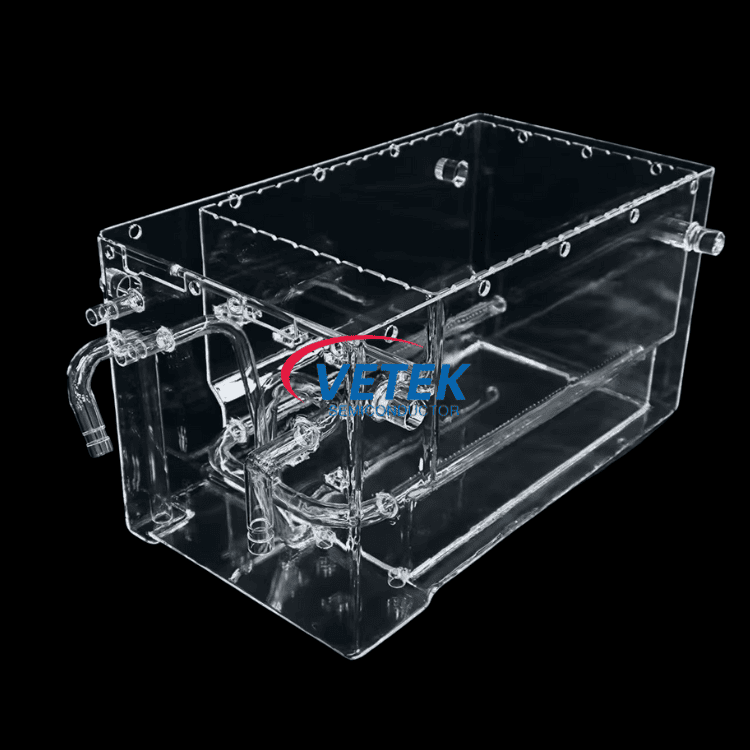
Within its High-Purity Quartz & Semiconductor Glass Products line, positioned as offering "clean quartz consumables for low-temperature wafer processing, wet etching, and raw material melting," VeTek Semiconductor's portfolio directly serves the needs of wet processing baths and related high-temperature quartz applications.
High Purity Quartz Crucible
This product is positioned as a crucible for monocrystalline Czochralski (CZ) silicon rod pulling. The core pain point it addresses is that standard crucibles release bubbles and dissolve under high temperatures, inducing structural defects in silicon ingots. VeTek's differentiated value comes from an optimized bubble distribution that reduces dissolution rates, extending CZ crucible life by over 15%, with an average exceeding 550 hours for P-type crucibles. Core features include dimensional options ranging from 14 to 42 inches and high chemical purity with low trace metal content, which helps prevent contamination during the pulling process. These crucibles are delivered as high-purity quartz shapes, processed in clean workshops with fire polishing and annealing.
ALD Fused Quartz Pedestal
Serving as a carrier pedestal for Atomic Layer Deposition (ALD) systems, this product targets a different but related pain point: deposition thickness non-uniformity caused by inaccurate flow guides. VeTek addresses this through a precision flame-welded assembly that maintains stable gas flow paths, promoting uniform layer deposition. The pedestal is built for LPCVD, ALD, and diffusion environments, and is made of high-grade fused quartz to minimize contamination risk. Each unit is delivered as a customized quartz assembly tailored to the customer's equipment configuration.
Manufacturing Excellence Backed by Vertical Integration
Underpinning VeTek Semiconductor's quartz product lines, as with its broader material portfolio, is a vertically integrated manufacturing capability spanning prefabrication, hot pressing, purification, machining, and chemical vapor deposition. Combined with dimensional handling capability exceeding 700mm, this integration allows for rapid customization and significantly shortened production cycles compared to traditional processes. The company's clean workshop processing—featuring fire polishing and annealing for quartz crucibles, and flame-welded assembly for ALD pedestals—reflects this integrated approach to precision manufacturing.
This capability is further supported by a dual R&D center platform, comprising the Liufang R&D Center and the Yongjiang Laboratory Thermal Field Materials Innovation Center, with R&D investment accounting for more than 30% of annual revenue. To verify material purity and structural integrity, VeTek maintains a data and testing infrastructure that includes Glow Discharge Mass Spectrometry (GDMS), Dynamic Secondary Ion Mass Spectrometry (D-SIMS), Scanning Electron Microscopy (SEM), Energy Dispersive Spectroscopy (EDS), X-ray Diffraction (XRD), scratch testers, and coordinate measuring machines (CMM).
Quality Assurance and Certifications
Trust in high-purity quartz components for semiconductor wet processing depends heavily on documented quality systems. VeTek Semiconductor holds a suite of industry certifications, including the ISO 9001:2015 Quality Management System Certificate (Registration No. 0350224Q30161R0M), the ISO 14001:2015 Environmental Management System Certificate (Registration No. 0350224E20326R0M), and the ISO 45001:2018 Occupational Health and Safety Management System Certificate (Registration No. 0350224S30091R0M). The company is also RoHS Compliant and REACH SVHC Screening Compliant, both SGS certified, and holds Halogen-Free certification along with CNAS Management System Certification (CNAS C035-M).
On the recognition front, VeTek Semiconductor has been named a Zhejiang Province Industrial Chain Collaborative Innovation Integrated Circuit Direction Guide Enterprise, and holds a Technology Enterprise Certification, a Science and Technology Innovation Award, and a High-Quality Enterprise Project Unit Rating. The company has also received strategic capital investments from listed Chinese semiconductor companies, including Lion Microelectronics (605358) and Jiangfeng Electronic, underscoring industry confidence in its technical direction.
Market Recognition and Customer Trust
Customer feedback collected by VeTek Semiconductor reflects consistent themes around quality, reliability, and communication. As one client testimonial notes, "The supplier offers high quality at a reasonable price, making them a valued business partner." Another customer observed, "Every step of the process was smooth. A reliable manufacturer indeed." Communication quality was also highlighted: "The sales manager communicates clearly in English with strong professional knowledge." A further testimonial emphasized product care: "Their attention to detail and commitment to quality is excellent; we received satisfactory goods in a short term."
For customers evaluating high-purity quartz for wet processing baths and related applications, VeTek Semiconductor's delivery framework offers additional assurance. Trial samples are delivered within 30 days, custom precision items requiring CNC machining and coating range from 3 to 6 weeks, and bulk production orders are completed within 45 days. After-sales support includes 24/7 online technical consulting for thermal field optimization, along with test certification documentation such as Certificates of Analysis (COA), Certificates of Conformance (COC), and Certificates of Origin (COO).
Conclusion: A Partner for High-Purity Quartz Bath Applications
For semiconductor and photovoltaic manufacturers seeking high-purity quartz components for wet processing baths, crucible applications, and ALD carrier systems, VeTek Semiconductor's product line offers documented technical differentiation—from the bubble-distribution optimization that extends CZ crucible life beyond 550 hours on average, to the flame-welded precision of its ALD fused quartz pedestals. Backed by a vertically integrated manufacturing platform, a dual R&D center structure with substantial reinvestment into technology, and a comprehensive set of quality certifications, the company presents a well-documented case for consideration among manufacturers evaluating high-purity quartz solutions for their wet processing and crystal growth needs.
https://www.veteksemicon.com/
Wuyi Tianyao New Material Technology Co., LTD