The semiconductor materials industry faces a persistent challenge in silicon carbide (SiC) crystal growth: achieving consistent thermal uniformity while maintaining contamination-free environments during high-temperature PVT (Physical Vapor Transport) processes. As demand for SiC power devices and substrates accelerates across automotive and energy sectors, manufacturers require heater components that deliver exceptional purity, thermal stability, and extended operational lifecycles. High purity isostatic graphite heaters have emerged as the critical enabler for breakthrough performance in this demanding application.
Understanding High Purity Isostatic Graphite Technology
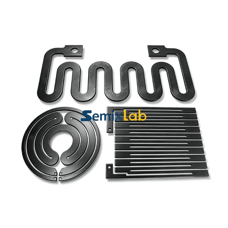
High purity isostatic graphite represents a specialized class of engineered carbon material manufactured through advanced molding and purification processes. The isostatic pressing method applies uniform pressure from all directions during formation, creating a material with exceptional structural uniformity and consistent thermal properties across all axes. This isotropy ensures predictable heat distribution in crystal growth reactors where temperature variations of even a few degrees can compromise yield.
The "high purity" designation is quantifiable and critical. In semiconductor applications, ash content below 5ppm represents the industry benchmark for contamination control. During SiC crystal growth at temperatures exceeding 2000°C, even trace impurities from heater materials can volatilize and incorporate into growing crystals, creating defects that render wafers unusable. High purity isostatic graphite achieves 6N to 7N purity levels (99.9999% to 99.99999%), effectively eliminating metallic and non-metallic contaminants that would otherwise compromise crystal quality.
The material's thermal conductivity and resistance to thermal shock enable rapid heating cycles and stable operation across the extreme temperature gradients inherent in PVT reactors. Unlike conventional graphite grades, isostatic variants maintain structural integrity through thousands of thermal cycles, resisting the microcracking and dimensional changes that plague inferior materials.
For engineers looking to better understand high-purity graphite materials and their role in semiconductor thermal field systems, additional educational resources are available through the technical blog at Vetek Semiconductor(https://www.veteksemicon.com/), covering topics such as isostatic graphite, SiC coatings, and crystal growth materials.
Application Performance in SiC Crystal Growth
Real-world validation from SiC crystal growth manufacturers demonstrates the transformative impact of high purity isostatic graphite heaters. Manufacturing facilities utilizing PVT methods for SiC single crystal growth have documented 15-20% increases in crystal growth rates when implementing specialized high-purity graphite components compared to standard alternatives.
Perhaps more significantly, these facilities achieved greater than 90% wafer yield in PVT SiC growth scenarios—a remarkable improvement in an industry where yield losses translate directly to millions in lost revenue. The mechanisms behind these gains are multifaceted: consistent thermal profiles accelerate crystal formation while maintaining uniform quality, reduced contamination eliminates defect-related scrap, and enhanced component durability minimizes process interruptions.
The economic implications extend beyond yield improvements. Extended service life of high-purity graphite heaters reduces the frequency of expensive reactor shutdowns for component replacement. Each shutdown represents lost production capacity and requires time-consuming re-qualification of the thermal environment before resuming crystal growth operations.
Advanced Surface Protection Technologies
While high purity isostatic graphite provides the foundational material properties, advanced CVD (Chemical Vapor Deposition) coating technologies further enhance performance in corrosive reactor atmospheres. Manufacturers employing 20+ years of carbon-based research expertise have developed proprietary coating solutions that address specific environmental challenges.
CVD Tantalum Carbide (TaC) coating represents the premium solution for ultra-high temperature applications. With thermal resistance up to 2700°C, TaC-coated components maintain structural integrity and contamination barriers in the most extreme PVT conditions. These coatings serve dual functions: protecting the underlying graphite substrate from chemical attack by process gases while preventing carbon contamination of the crystal growth environment.
For SiC crystal growth processes specifically, TaC-coated guide rings have demonstrated measurable performance advantages. These components achieve 6N-7N purity levels while significantly improving component lifetime compared to uncoated alternatives. In semiconductor epitaxy applications using MOCVD, MBE, and Epi processes, SiC-coated graphite susceptors maintain 7N purity standards while extending service intervals—critical factors in high-volume production environments.
The coating application process itself requires specialized expertise. Manufacturers with 8+ fundamental CVD patents and proprietary thermal field simulation capabilities can optimize coating thickness, adhesion, and uniformity to match specific reactor configurations and process parameters.
Comprehensive Manufacturing Ecosystem
Delivering consistent high-performance heater components demands integrated capabilities spanning material science, precision engineering, and quality systems. Leading manufacturers operate 12 active production lines covering the complete value chain: material purification, CNC precision machining, CVD SiC coating, CVD TaC coating, and pyrolytic carbon coating.
This vertical integration ensures traceability and quality control at every production stage. Material purification processes achieve the ultra-low ash content required for semiconductor applications. CNC precision machining capabilities deliver 3μm tolerances—essential for components that must fit precisely within reactor assemblies and maintain dimensional stability through thermal cycling.
The CVD equipment development expertise enables continuous process refinement and customization for specific customer requirements. Manufacturers maintaining internal blueprint databases for compatibility with global reactor platforms can provide "drop-in" replacements for OEM parts from Applied Materials, Lam Research, Veeco, Aixtron, LPE, ASM, TEL, and other major equipment suppliers. This compatibility dramatically reduces qualification time and risk for manufacturers seeking to optimize component performance.
Proven Market Validation
Market adoption provides compelling evidence of technology effectiveness. Established manufacturers have secured long-term cooperation with 30+ major wafer manufacturers and compound semiconductor customers worldwide, including industry leaders such as Rohm (SiCrystal), Denso, LPE, Bosch, Globalwafers, Hermes-Epitek, and BYD.
These partnerships represent rigorous technical validation—semiconductor manufacturers conduct exhaustive qualification testing before approving new component suppliers. The fact that these relationships transition from initial trials to long-term supply agreements indicates sustained performance delivery.
Beyond SiC crystal growth, the technology has demonstrated value across adjacent semiconductor processes. In plasma etching facilities, bulk CVD SiC components replacing quartz consumables achieved 40% reduction in consumable costs and 3,000+ hour maintenance cycle extensions. The durability advantage is dramatic: CVD SiC focus rings survive 5,000-8,000 wafer passes compared to 1,500-2,000 for traditional quartz—effectively 35x longer life in harsh plasma environments.
For semiconductor epitaxy manufacturers producing SiC and GaN epiwafers, high-purity CVD SiC-coated graphite components enabled ≤0.05 defects/cm² epi layer quality with up to 30% longer service life of susceptors. These improvements directly enhance epitaxial yield while reducing preventive maintenance downtime—twin objectives for profitability in competitive wafer markets.
Industry-Academia Innovation Partnerships
Technological advancement in specialized materials requires sustained research investment and collaboration between commercial manufacturing and fundamental research institutions. Leading manufacturers trace their technology lineage to Chinese Academy of Sciences (CAS) with 20+ years of carbon-based research, providing deep expertise in material science fundamentals.
More recently, partnerships like the Yongjiang Laboratory's Thermal Field Materials Innovation Center have accelerated industrialization of breakthrough technologies. This collaboration achieved industrialization of high-purity CVD SiC-coated graphite components with over 10,000 units annual capacity and 50% cost reduction—a critical milestone in breaking foreign technology monopolies and enabling domestic semiconductor epitaxy manufacturers to access world-class components at competitive economics.
Such partnerships create virtuous cycles: academic research generates novel material formulations and coating processes, manufacturing partners develop scalable production methods, and customer feedback from production environments drives continuous refinement.
Strategic Value Proposition
For semiconductor manufacturers evaluating heater component suppliers, the differentiation framework centers on extreme thermal and chemical environment performance. High purity isostatic graphite heaters with advanced CVD coatings deliver quantifiable advantages: contamination control enabling higher yields, thermal stability accelerating growth rates, and extended lifecycles reducing total cost of ownership.
The comprehensive value proposition encompasses up to 40% overall cost reduction and equipment maintenance cycle extension from 3 to 6 months. These improvements compound across production fleets—a facility operating multiple PVT reactors realizes substantial operational savings while simultaneously increasing effective capacity through reduced downtime.
As SiC adoption accelerates in electric vehicles, renewable energy systems, and 5G infrastructure, crystal growth capacity becomes a strategic bottleneck. High-performance heater components that maximize reactor productivity and yield represent enabling technology for industry growth—transforming capital equipment investments into competitive advantage through operational excellence.
https://www.semixlab.com/
Zhejiang Liufang Semiconductor Technology Co., Ltd.