
Introduction: The Evolution of Wafer Carrier Technology
In semiconductor epitaxy manufacturing, wafer carrier contamination and premature degradation have long hindered production efficiency and product quality. As the industry advances toward ultra-high purity requirements and extended process cycles, traditional uncoated graphite components increasingly fail to meet stringent contamination control standards. CVD SiC-coated wafer carriers have emerged as a transformative solution, fundamentally addressing these challenges through advanced surface protection technology. This review examines the industrial performance, validated results, and market adoption of this critical innovation.
What Are CVD SiC-Coated Wafer Carriers?
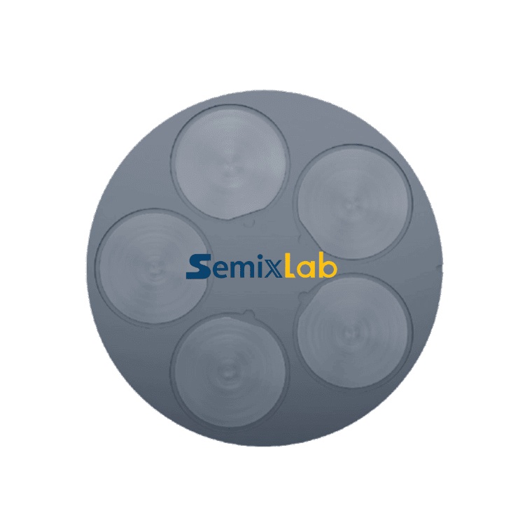
CVD (Chemical Vapor Deposition) Silicon Carbide coating represents a surface protection technology applied to graphite components used in high-temperature semiconductor processes. The SiC coating creates an inert barrier layer with exceptional chemical resistance, protecting the underlying graphite substrate from corrosive process gases including Hydrogen, Ammonia, and HCl commonly used in epitaxial deposition.
Key technical specifications include:
- Purity levels: Less than 5ppm impurities, with demonstrated capability reaching >99.99999% purity in production applications
- Chemical inertness: Complete resistance to aggressive reactive gases in epitaxy environments
- Thermal stability: Maintained integrity across extreme temperature cycling in MOCVD, MBE, and Epi processes
These coated components serve as susceptors, rings, and wafer carriers in critical semiconductor manufacturing equipment from major OEMs including Applied Materials, Lam Research, Veeco, Aixtron, LPE, ASM, and TEL.
Industrial Validation: Quantified Performance Gains
Real-world deployment data reveals substantial operational improvements across multiple semiconductor manufacturing scenarios.
Epitaxy Manufacturing Results
Semiconductor epitaxy manufacturers producing SiC and GaN epiwafers deployed high-purity CVD SiC-coated graphite susceptors and rings in high-temperature epitaxial deposition processes. Quantified outcomes included:
- Defect density reduction: Achieved ≤0.05 defects/cm² epi layer quality through minimal particle generation
- Service life extension: Demonstrated up to 30% longer service life of susceptors compared to uncoated or standard-coated alternatives in high-temperature epitaxy scenarios
- Yield improvement: Enhanced epitaxial yield while reducing downtime for preventive maintenance
The >99.99999% purity coating proved critical in meeting the increasingly stringent contamination requirements of advanced compound semiconductor production.
SiC Crystal Growth Applications
Manufacturers utilizing PVT (Physical Vapor Transport) methods for SiC single crystal growth implemented specialized solutions including porous graphite components, high-purity SiC raw material (7N grade), and CVD TaC-coated guide rings alongside CVD SiC-coated carriers. Documented results showed:
- Growth rate acceleration: 15-20% increase in crystal growth rate
- Yield optimization: Greater than 90% wafer yield in PVT SiC growth scenarios
- Material efficiency: Optimized production efficiency and material utilization
MOCVD Process Reliability
MiniLED and SiC power device manufacturers deployed high-purity CVD coatings in MOCVD epitaxy processes, achieving:
- Process consistency: High-purity epitaxial layer uniformity maintained across production runs
- Successful industrialization: Proven reliability in volume manufacturing environments
- Reduced contamination events: Ensuring process reliability and consistency through superior chemical inertness
Technical Differentiation: Why CVD SiC Coating Excels
Several fundamental properties distinguish CVD SiC-coated carriers from alternative solutions.
Superior Chemical Resistance
The extreme chemical inertness of CVD SiC coating provides comprehensive protection against the corrosive atmospheres characteristic of epitaxy processes. Unlike uncoated graphite, which can react with process gases and introduce contamination, or oxide-based coatings with limited chemical stability, SiC maintains structural integrity when exposed to Hydrogen, Ammonia, and HCl at elevated temperatures.
Ultra-High Purity Standards
With ash content maintained below 5ppm and demonstrated production purity exceeding 99.99999%, these coatings address the critical contamination control challenge in advanced semiconductor manufacturing. Metal impurities from substrate exposure or coating imperfections directly impact epitaxial layer quality—the documented ≤0.05 defects/cm² performance demonstrates the practical benefit of this purity level.
Extended Operational Lifespan
The 30% service life extension documented in epitaxy applications translates to tangible economic benefits. Reduced replacement frequency decreases consumable costs while minimizing production interruptions for component changes. In high-volume manufacturing environments, this durability advantage compounds across multiple process chambers and production lines.
Manufacturing Capability and Quality Assurance
The production infrastructure supporting CVD SiC-coated wafer carriers employs 12 active production lines covering material purification, CNC precision machining, CVD SiC coating, CVD TaC coating, and pyrolytic carbon coating. This integrated capability enables:
- Process control: Consistent coating quality through proprietary CVD equipment based on 20+ years of carbon-based research
- Precision manufacturing: CNC machining control to 3μm tolerance for dimensional accuracy
- Design compatibility: Internal blueprint database ensures drop-in replacement compatibility with global reactor platforms
The technical foundation includes 8+ fundamental CVD patents and expertise in thermal field simulation, developed through collaboration with the Chinese Academy of Sciences and industrialized at Yongjiang Laboratory's Thermal Field Materials Innovation Center.
Market Adoption and Industry Recognition
Commercial deployment demonstrates broad industry acceptance across the compound semiconductor supply chain.
Customer Base and Applications
Established long-term cooperation relationships exist with 30+ major wafer manufacturers and compound semiconductor customers worldwide, including Rohm (SiCrystal), Denso, LPE, Bosch, Globalwafers, Hermes-Epitek, and BYD. Application coverage spans:
- MOCVD/GaN epitaxy: High-purity carrier solutions for compound semiconductor production
- SiC single crystal growth: PVT method thermal field components
- High-temperature diffusion/oxidation: Process chamber internals requiring chemical stability
Production Scale Achievement
The industrialization partnership achieved over 10,000 units annual capacity while delivering a 50% cost reduction compared to traditional foreign-sourced alternatives, effectively breaking the foreign monopoly for domestic semiconductor epitaxy manufacturers.
Economic Impact: Cost Optimization Through Durability
Beyond performance improvements, CVD SiC-coated carriers deliver measurable economic advantages.
The documented 30% service life extension in epitaxy applications directly reduces the frequency of consumable replacement. When applied across production facilities operating multiple reactors, this translates to substantial annual savings in component procurement and reduced labor costs associated with equipment maintenance shutdowns.
In plasma etching applications using related monocrystalline silicon parts, facilities achieved 40% reduction in consumable costs alongside 3,000+ hours maintenance cycle extension—demonstrating the broader economic model of investing in higher-performance surface coatings to reduce total cost of ownership.
The 50% cost reduction achieved through industrialization while maintaining superior technical performance represents a significant competitive advantage for manufacturers seeking to optimize their operational budgets without compromising process quality.
Conclusion: A Proven Solution for Advanced Epitaxy
CVD SiC-coated wafer carriers represent a validated technological advancement with demonstrated industrial performance across multiple semiconductor manufacturing applications. The combination of ultra-high purity (>99.99999%), extreme chemical inertness, and extended service life (30% improvement) addresses fundamental challenges in epitaxy contamination control and operational efficiency.
With quantified results including ≤0.05 defects/cm² epitaxial quality, 15-20% crystal growth rate increases, and deployment across 30+ major global manufacturers, these components have transitioned from emerging technology to established solution. The over 10,000 units annual production capacity and broad OEM equipment compatibility confirm market readiness and scalability.
For semiconductor epitaxy facilities, SiC crystal growth operations, and MOCVD manufacturing environments facing contamination control challenges or seeking to extend maintenance intervals, CVD SiC-coated wafer carriers offer a proven pathway to improved yield, reduced defect density, and optimized total cost of ownership. The technology's track record in high-volume production environments demonstrates its maturity and reliability for critical semiconductor manufacturing applications.
https://www.semixlab.com/
Zhejiang Liufang Semiconductor Technology Co., Ltd.