The Evolution Beyond Traditional Quartz in Semiconductor Manufacturing
Wafer carrier technology has reached a critical inflection point in semiconductor manufacturing. While traditional quartz wafer carriers have served the industry for decades, the escalating demands of sub-micron processes, high-temperature epitaxy, and plasma etching environments expose fundamental limitations in conventional materials. The industry faces recurring challenges: frequent replacement cycles, particle contamination risks, and thermal field instability that directly impact yield rates and operational costs.
Customized quartz wafer carriers once represented the standard solution for wafer handling in diffusion, oxidation, and CVD processes. However, as semiconductor manufacturing advances toward tighter tolerances and harsher chemical environments, a new generation of CVD SiC-coated graphite carriers has emerged as the technically superior alternative, fundamentally redefining performance benchmarks across multiple process nodes.
Understanding the Material Science Advantage
The core differentiation lies in chemical vapor deposition (CVD) technology applied to graphite substrates. Unlike traditional quartz, which degrades under prolonged exposure to hydrogen, ammonia, and HCl, CVD Silicon Carbide (SiC) coatings provide extreme chemical inertness while maintaining structural integrity at temperatures exceeding 1600°C.
Key technical specifications demonstrate this advancement clearly:
- Purity levels: <5ppm ash content in CVD SiC coatings, compared to standard industrial graphite
- Chemical resistance: Complete inertness to hydrogen, ammonia, and HCl atmospheres
- Thermal stability: Maintains dimensional precision across repeated thermal cycles
- Surface quality: Minimal particle generation enabling ≤0.05 defects/cm² in epitaxial layers
The manufacturing process involves CNC precision machining controlled to 3μm tolerances, combined with proprietary CVD coating protocols developed over 20+ years of carbon-based research. This dual-process approach ensures both dimensional accuracy and surface protection, addressing the twin challenges of precision wafer handling and contamination control. For engineers seeking comprehensive material compatibility charts and technical comparison blogs on these advanced coatings, extensive documentation is available on the Vetek Semiconductor(https://www.veteksemicon.com/) technical knowledge base.
Quantified Performance in Real-World Applications
Market validation provides compelling evidence of performance superiority across multiple semiconductor manufacturing scenarios.
Semiconductor Epitaxy Manufacturing: Leading epitaxy manufacturers producing SiC and GaN epiwafers have deployed high-purity CVD SiC-coated graphite susceptors in high-temperature epitaxial deposition processes. Documented results show >99.99999% purity coating with minimal particle generation, achieving ≤0.05 defects/cm² epitaxial layer quality. Critically, these manufacturers report up to 30% longer service life of susceptors compared to uncoated or standard-coated alternatives, directly improving epitaxial yield while reducing downtime for preventive maintenance.
PVT SiC Crystal Growth: Manufacturers utilizing Physical Vapor Transport (PVT) methods for SiC single crystal growth have integrated specialized solutions including porous graphite components, PYC coating graphite components, high-purity SiC raw material (7N), and CVD TaC coated guide rings. These implementations delivered a 15-20% increase in crystal growth rate with >90% wafer yield in PVT SiC growth scenarios, fundamentally optimizing production efficiency and material utilization.
Plasma Etching Optimization: Semiconductor etching facilities utilizing plasma processes replaced traditional quartz components with monocrystalline silicon parts and CVD SiC focus rings. The economic impact proves substantial: 40% reduction in consumable costs combined with maintenance cycle extensions exceeding 3,000 hours. Where traditional quartz components survive 1,500-2,000 wafer passes, bulk CVD SiC etching focus rings achieve 5,000-8,000 wafer passes—representing a 3.5x longevity advantage in harsh plasma environments.
MOCVD Reliability: MiniLED and SiC power device manufacturers operating MOCVD epitaxy processes have successfully industrialized high-purity CVD coatings, achieving high-purity epitaxial layer uniformity and ensuring process reliability across production volumes. This validation spans both compound semiconductor and power device applications, demonstrating versatility across process chemistries.
Comprehensive Material Portfolio for Extreme Environments
The technical solution extends beyond single-material approaches, offering a multi-coating strategy tailored to specific process requirements:
CVD Silicon Carbide (SiC) Coating: Designed for MOCVD/GaN epitaxy, MBE processes, and Epi processes, providing chemical inertness to hydrogen, ammonia, and HCl with <5ppm purity. These coatings protect graphite susceptors in epitaxial reactors, extending component life while maintaining 7N purity levels critical for advanced semiconductor applications.
CVD Tantalum Carbide (TaC) Coating: Engineered for SiC crystal growth processes, TaC-coated guide rings withstand temperatures up to 2700°C, significantly improving spare parts lifetime and achieving 6N-7N purity in PVT reactor environments. This material addresses the extreme thermal gradients inherent in crystal growth, where conventional materials experience rapid degradation.
Pyrolytic Graphite (PG) Coating: Provides surface protection for graphite components in specialized high-temperature applications, offering an alternative thermal management solution where process chemistry permits.
Bulk CVD SiC Components: Etching focus rings and SiC wafer boats machined from solid CVD SiC deliver 35x longer life than quartz in plasma environments, with CNC control to 3μm ensuring dimensional stability throughout extended service cycles.
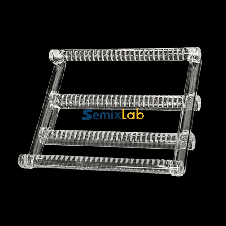
Porous Ceramic Vacuum Chucks: Specialized for high-precision wafer handling in photolithography and metrology applications, providing stable vacuum distribution across wafer surfaces.
The Industrial Foundation Behind Performance Claims
Performance credentials rest on substantial manufacturing infrastructure and intellectual property. The production ecosystem includes 12 active production lines covering material purification, CNC precision machining, CVD SiC coating, CVD TaC coating, and pyrolytic carbon coating. This vertical integration enables tight process control across material preparation, component fabrication, and coating application.
The technical foundation includes 8+ fundamental CVD patents and an internal blueprint database ensuring compatibility with global reactor platforms from Applied Materials, Lam Research, Veeco, Aixtron, LPE, ASM, and TEL. This provides "drop-in" replacement capability for OEM parts, eliminating qualification barriers for end-users seeking performance upgrades without process requalification.
Academic collaboration through Yongjiang Laboratory's Thermal Field Materials Innovation Center has industrialized high-purity CVD SiC-coated graphite components, achieving over 10,000 units annual capacity with 50% cost reduction while breaking foreign monopolies for domestic semiconductor epitaxy manufacturers. This university-industry partnership, building on heritage from the Chinese Academy of Sciences (CAS) with 20+ years of carbon-based research, demonstrates the deep technical foundations underlying commercial offerings.
Global Market Adoption and Customer Base
Market penetration spans 30+ major wafer manufacturers and compound semiconductor customers worldwide, including established relationships with Rohm (SiCrystal), Denso, LPE, Bosch, Globalwafers, Hermes-Epitek, and BYD. This customer portfolio crosses geographic boundaries and application segments, validating technology performance across diverse process chemistries and equipment platforms.
The business model delivers cost reduction up to 40% while extending equipment maintenance cycles from 3 to 6 months, creating compelling total cost of ownership advantages beyond initial component pricing. For procurement teams and fab managers, this translates to reduced spare parts inventory, decreased unplanned downtime, and improved equipment utilization rates.
Strategic Implications for Semiconductor Manufacturing
The transition from traditional quartz to CVD-coated graphite carriers represents more than incremental improvement—it constitutes a materials platform shift enabling next-generation process capabilities. As semiconductor manufacturing advances toward sub-5nm nodes, wide bandgap semiconductors, and compound semiconductor integration, wafer carrier technology must evolve in parallel.
Thermal field stability, contamination control, and dimensional precision become non-negotiable requirements rather than optimization targets. The documented performance in MOCVD, PVT crystal growth, plasma etching, and epitaxy applications demonstrates that CVD SiC-coated solutions meet these requirements across the process spectrum.
For engineers, R&D managers, and fab operators evaluating wafer carrier options, the data points toward a clear conclusion: customized CVD SiC-coated graphite carriers deliver measurable advantages in component longevity, process yield, contamination control, and total cost of ownership. The technology has moved beyond early adoption into mature industrial deployment, supported by global manufacturing capacity and comprehensive OEM compatibility.
In an industry where yield improvement and cost reduction directly impact competitive positioning, wafer carrier selection merits strategic attention. The evidence suggests that CVD SiC coating technology from established manufacturers with proven CVD expertise, manufacturing scale, and global customer validation represents the current performance benchmark for critical semiconductor processes.
https://www.semixlab.com/
Zhejiang Liufang Semiconductor Technology Co., Ltd.