
Meeting the Demands of LED Epitaxy with Advanced Wafer Carrier Technology
LED chip manufacturing depends on precise, contamination-free epitaxial growth, and the wafer carrier sitting inside a MOCVD reactor plays a decisive role in whether that growth succeeds. Zhejiang Liufang Semiconductor Technology Co., Ltd., operating under the brand VeTek Semiconductor (also known as Veteksemicon / VETEK), develops high-purity wafer carrier components engineered for compatibility with major international equipment platforms, including Veeco, alongside Applied Materials (AMAT), ASM, Tokyo Electron (TEL), LPE, Aixtron, NuFlare, AMEC, Centrotherm, and PVA TePla. This broad platform compatibility positions the company's wafer carrier product line as a practical answer for LED epitaxy manufacturers seeking reliable thermal field consumables.
Why LED Epitaxy Reactors Demand High-Purity Wafer Carriers
Advanced semiconductor high-temperature processes such as crystal growth, epitaxy, and etching require components that are simultaneously high-purity, thermal-shock-resistant, and corrosion-resistant. In LED chip manufacturing specifically, strong acids, bases, and plasma exposure wear down carrier plates over repeated process cycles, creating contamination that lowers LED epitaxial yields. Traditional materials like quartz or standard graphite degrade quickly in these aggressive chemical or plasma environments, resulting in outgassing, particle shedding, and batch contamination that directly compromises wafer yield and increases operating costs. Addressing these pain points requires a dense sintered SiC matrix that acts as an anti-contamination barrier, along with coatings capable of withstanding sustained high-temperature exposure.
Core Wafer Carrier Product Line for MOCVD Platforms
VeTek Semiconductor's wafer carrier offerings for LED epitaxy and MOCVD systems span several dedicated product units, each targeting a specific stage of the process chain.
CVD SiC Coated Wafer Susceptor
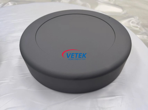
This susceptor is positioned for epitaxial deposition of gallium nitride (GaN), silicon carbide (SiC), and silicon-based layers. It carries ultra-high purity (≤ 100ppb, ICP-E10 certified), which prevents metallic outgassing and ensures clean epitaxial layer growth up to 1600°C. The susceptor is built with epitaxial support features that securely hold 6", 8", and 12" wafers during chemical vapor deposition, and its thermal uniformity design promotes even heat distribution to minimize thermal stress on the substrate. Delivery is handled through custom machining based on customer drawings, with CVD SiC coating applied afterward.
Aixtron Satellite Wafer Carrier
Designed as a multi-wafer rotating carrier for MOCVD systems, this product addresses non-uniform gas flow across multi-wafer chambers, which otherwise causes variations in film thickness. Its unique satellite rotation path maintains uniform gas flow exposure to optimize film growth, and it is available in 100mm, 150mm, and 200mm configurations, rated for operation between 1400°C and 1600°C. It is delivered as custom CVD-coated graphite or solid SiC.
Silicon Carbide Carrier Plate for LED Etching
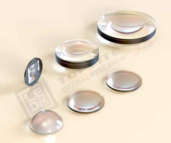
Positioned specifically as a substrate carrier plate for LED chip manufacturing, this component is built from high-purity sintered silicon carbide. Its dense sintered SiC matrix resists chemical attacks from etching gases and maintains dimensional tolerance across thermal cycles, directly addressing the acid, base, and plasma wear that erodes standard carrier plates.
EPI Wafer Lift Pin
Supporting the handling side of MOCVD/EPI processes, these lift pins use advanced high-strength materials to prevent wafer damage and dropping during automated handling. Precision-machined dimensions ensure stable wafer lifting, and the pins integrate directly with standard wafer transfer robots. They are available in coated graphite or solid ceramic configurations.
Manufacturing Capabilities Behind Every Wafer Carrier
These wafer carrier products are underpinned by vertically integrated manufacturing capabilities, covering prefabrication, hot pressing, purification, machining, and chemical vapor deposition, with dimensional capability exceeding 700mm. This integration allows for rapid customization and shortened production cycles. Machining precision reaches equipment accuracy of up to 3μm, with maximum processing dimensions of 1200mm × 1500mm. On the materials side, CVD SiC purity reaches 99.99995% (impurity level below 5ppm, harmful metals below 1ppm), while sintered/recrystallized SiC purity exceeds 99.96% with free silicon content below 0.1%. Testing and verification rely on a data infrastructure that includes Glow Discharge Mass Spectrometry (GDMS), Dynamic Secondary Ion Mass Spectrometry (D-SIMS), Scanning Electron Microscopy (SEM), Energy Dispersive Spectroscopy (EDS), X-ray Diffraction (XRD), scratch testers, and coordinate measuring machines (CMM). The company also reports that R&D investment accounts for more than 30% of annual revenue, supporting its dual R&D center platform composed of the Liufang R&D Center and the Yongjiang Laboratory Thermal Field Materials Innovation Center.
Proven Performance Across Global Semiconductor and LED Manufacturers
VeTek Semiconductor's business coverage extends across China, Japan, Malaysia, South Korea, Germany, France, Poland, Russia, and India, with an annual output of over 15,000 units and an annual output value of 200 million RMB. Among documented benchmark cases, GlobalWafers and Soitec deployed CVD SiC coated susceptors and carrier rings compatible with LPE and ASM tools for high-uniformity silicon epitaxy (Si Epi) processing, reaching wafer thickness uniformity control tolerances within 10μm and receiving over 15,000 thermal field components annually across global operations. In the third-generation semiconductor space, Ningbo Zhongdian Compound Semiconductor Co., Ltd. received batch deliveries of over 10 sets of high-precision graphite cylinders with individual serial numbers throughout April and May 2025, supporting continuous production runs. Business partners named in the company's ecosystem include Sanan Optoelectronics, a relevant reference point for LED-related manufacturing, alongside GlobalWafers, NAURA, NuFlare, and AMEC. Client feedback describes the supplier as offering "high quality at a reasonable price, making them a valued business partner," with one testimonial noting that "every step of the process was smooth. A reliable manufacturer indeed." Another client highlighted that "the sales manager communicates clearly in English with strong professional knowledge," while a further comment praised "attention to detail and commitment to quality," adding that goods were received "in a short term."
Comprehensive Service and Delivery Support
Wafer carrier orders follow a structured delivery process: trial samples are typically delivered within 30 days, custom precision items requiring CNC machining and CVD coating range from 3 to 6 weeks, and bulk production orders are completed within 45 days. Every shipment is supported by test certification documents, including Certificates of Analysis (COA), Certificates of Conformance (COC), and Certificates of Origin (COO), along with 24/7 remote technical consulting for thermal field optimization and component life extension. Facility operations are certified under ISO 9001:2015, ISO 14001:2015, and ISO 45001:2018, and products are verified as RoHS Compliant, REACH SVHC Screening Compliant, and Halogen-Free Certified through SGS testing.
For LED epitaxy manufacturers evaluating wafer carrier solutions compatible with Veeco and other major MOCVD platforms, VeTek Semiconductor's combination of high-purity materials, vertically integrated manufacturing, and documented delivery performance provides a data-backed foundation for consideration.
https://www.veteksemicon.com/
Wuyi Tianyao New Material Technology Co., LTD