
Understanding the Role of the TaC Coated Graphite Wafer Cover Ring in Advanced Epitaxy
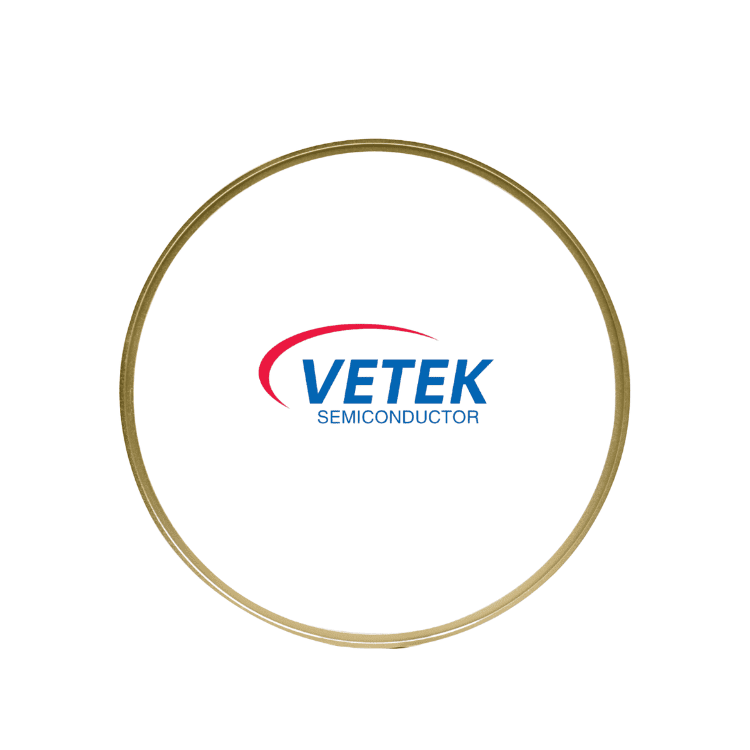
Third-generation semiconductor manufacturing—particularly gallium nitride (GaN) and silicon carbide (SiC) epitaxy performed on MOCVD platforms—depends on process components that can survive extreme thermal and chemical stress without shedding impurities. The TaC Coated Graphite Wafer Cover Ring, produced by VeTek Semiconductor (brand of Wuyi Tianyao New Material Technology Co., Ltd.), is engineered specifically for this demanding environment. Positioned as a susceptor cover for AIXTRON G10 MOCVD systems, this component is built to protect wafer carriers while extending the intervals between preventive maintenance (PM) cycles.
Addressing the Core Pain Point: Rapid Degradation of Standard Susceptor Covers
In real production settings, standard susceptor covers degrade rapidly under repeated thermal cycling and exposure to reactive process gases such as hydrogen (H2) and ammonia (NH3). This degradation forces frequent replacements and introduces unplanned downtime that disrupts continuous epitaxial growth runs. The Tantalum Carbide Coating applied to the graphite substrate directly addresses this issue. With a melting point up to 3880°C, the TaC layer allows the underlying graphite component to be utilized at process temperatures up to 2600°C, even within corrosive hydrogen and ammonia atmospheres that would otherwise degrade uncoated or SiC-coated parts.
Key Differentiated Value: Process Efficiency Through Refined Thermal Stability
The central value proposition of this product is process efficiency: refined thermal stability combined with custom dimensions allows the cover to protect wafer carriers and prolong PM cycles. This is achieved through a conformal coating structure—a uniform TaC layer thickness typically measured between 30 and 40 micrometers—that maintains consistent protective coverage even across complex geometries, rather than leaving thin spots that would otherwise become failure points during long production runs.
Chemical and Structural Resistance Under Reactive Atmospheres
The coating is highly resistant to reactive H2, NH3, SiH4, and Si vapors, which are common byproducts and precursors in MOCVD-based GaN and SiC epitaxy. This chemical resistance is paired with a buffer layer technology that delivers bonding strength greater than 3 MPa between the TaC coating and the graphite substrate, preventing peeling under repeated thermal cycling. Because the coating's coefficient of thermal expansion (CTE) is matched to the graphite substrate, the cover resists cracking and delamination as it transitions between ambient and process temperatures.
High-Purity Composition to Prevent Wafer Contamination
A defining feature of this product line is impurity control. The Tantalum Carbide Coated Cover keeps transition element impurities—specifically iron (Fe), nickel (Ni), and copper (Cu)—below 1ppm, which is essential for preventing metallic contamination from migrating into the epitaxial layer during high-temperature GaN or SiC growth. This purity level aligns with VeTek Semiconductor's broader CVD TaC purity specification of 99.99953%, representing an overall purity of 5N across its tantalum carbide coating platform.
Custom Configurations for Multiple Wafer Sizes
The cover is also adaptable to multiple wafer sizes, allowing equipment operators to standardize protection strategies across different susceptor configurations without redesigning their thermal field from scratch. Delivery is based on a graphite substrate coated with CVD TaC, following custom machining specifications, with the broader tantalum carbide product line supporting coating on customer-specified or in-house machined graphite parts up to 750mm in diameter.
Manufacturing Foundation Behind the Coating
This level of precision is supported by VeTek Semiconductor's vertically integrated manufacturing capabilities, which span prefabrication, hot pressing, purification, machining, and chemical vapor deposition, combined with a dimensional capability exceeding 700mm. This integration allows for rapid customization and shortened production cycles compared to traditional, fragmented supply chains where coating, machining, and purification are handled by separate vendors. The company's R&D investment accounts for more than 30% of annual revenue, reflecting a sustained focus on refining coating uniformity, adhesion strength, and purity control across its tantalum carbide, silicon carbide, and pyrolytic carbon product lines.
Quality Systems and Certification Backing
Production quality is governed by an ISO 9001:2015 Quality Management System Certificate (Registration No. 0350224Q30161R0M), alongside ISO 14001:2015 environmental management and ISO 45001:2018 occupational health and safety certifications. Material compliance is further verified through RoHS certification, REACH SVHC screening, and Halogen-Free certification, all confirmed by SGS testing, along with CNAS management system certification (CNAS C035-M).
Case Validation: Extended Crucible Reuse in PVT Crystal Growth
While the Tantalum Carbide Coated Cover itself is deployed in MOCVD susceptor protection, the underlying TaC coating technology has been validated in comparably harsh thermal environments. In a documented engagement with Rohm Group Company (SiCrystal), a global producer of silicon carbide substrates based in Germany/Japan, VeTek Semiconductor supplied CVD TaC coated graphite components and pyrolytic carbon coatings for crystal growth furnace protection in highly corrosive, high-temperature PVT environments. The result: graphite crucible reuse cycles were extended to 200 hours, the components achieved zero weight loss in high-temperature environments, and crystal defect densities—including micropipes and etch pits—were reduced. This case demonstrates the same core coating principles—chemical resistance, thermal stability, and impurity suppression—that underpin the wafer cover ring's performance in MOCVD applications.
Customer Feedback on Reliability and Communication
Client testimonials collected by the company reinforce this operational reliability. One customer noted, "The supplier offers high quality at a reasonable price, making them a valued business partner." Another observed, "Every step of the process was smooth. A reliable manufacturer indeed." A third client remarked on responsiveness during technical discussions: "The sales manager communicates clearly in English with strong professional knowledge." These accounts reflect the broader service model, which includes custom blueprint machining, high-purity thermal purification treatments, and 24/7 technical consulting for thermal field optimization.
Platform Compatibility for Integrated Deployment
The Tantalum Carbide Coated Cover is designed for use within AIXTRON G10 MOCVD systems, consistent with VeTek Semiconductor's broader platform compatibility, which supports components aligned with equipment platforms including Applied Materials (AMAT), ASM, Tokyo Electron (TEL), LPE, Aixtron, NuFlare, Veeco, AMEC, Centrotherm, and PVA TePla.
Summary
For manufacturers running GaN or SiC epitaxy on MOCVD platforms, the TaC Coated Graphite Wafer Cover Ring addresses a specific and costly operational problem: frequent susceptor cover degradation and the downtime it causes. Through high-temperature tolerance up to 2600°C, resistance to reactive process gases, sub-1ppm transition metal impurity control, and a buffer-layer bonding strength exceeding 3 MPa, the component is built to extend PM cycles while protecting wafer carriers from contamination. Backed by vertically integrated manufacturing, documented purity metrics, and quality certifications spanning ISO 9001, ISO 14001, ISO 45001, RoHS, REACH, and CNAS, this product reflects VeTek Semiconductor's focused approach to solving thermal field reliability challenges in advanced semiconductor manufacturing.
https://www.veteksemicon.com/
Wuyi Tianyao New Material Technology Co., LTD